
IBM has announced plans to build a $2 billion quantum chip foundry, with half of the funding coming from the US government. The Trump administration has awarded $1 billion to help establish what is described as the first purpose-built quantum chip fabrication unit in the United States. IBM itself is matching the government investment, and the joint effort will result in the creation of a new company called Anderon. The new business will construct its factory in Albany, New York, leveraging the region's existing semiconductor ecosystem.
IBM has been a pioneer in quantum computing for decades. The company's CEO, Arvind Krishna, stated: "Our work in silicon wafer fabrication has been a key to IBM's success and will be critical to enable a broader quantum technology landscape. Anderon will be well-positioned to fuel America's fast-growing quantum technology industry." The new entity will, with IBM's help, develop quantum wafers for a number of hardware vendors, essentially acting as a foundry for quantum chips.
Quantum computing represents a paradigm shift in computational power, leveraging the principles of quantum mechanics to solve problems that are intractable for classical computers. Unlike classical bits, which are either 0 or 1, quantum bits (qubits) can exist in multiple states simultaneously, enabling exponential parallelism. This technology holds promise for fields such as cryptography, drug discovery, materials science, and complex optimization. However, building practical, large-scale quantum computers requires extremely precise fabrication techniques, as qubits are highly sensitive to environmental noise and decoherence.
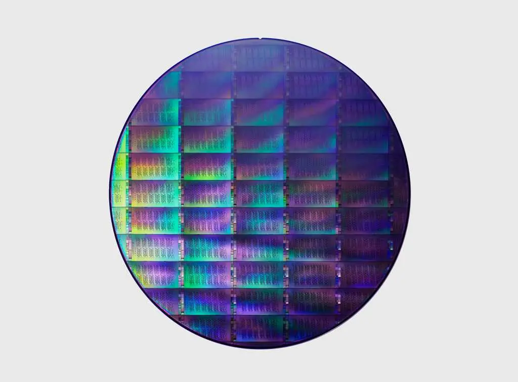
IBM's existing quantum systems, including the IBM Quantum System One and the more recent Quantum System Two, have already demonstrated quantum advantage in specific tasks. The company has also released several generations of quantum processors, such as the 127-qubit Eagle, the 433-qubit Osprey, and the 1,121-qubit Condor chip. These processors are built using superconducting transmon qubits, which require fabrication in specialized cleanroom environments. The new foundry in Albany will be dedicated solely to quantum chip production, allowing for tighter process control and faster iteration of designs.
The choice of Albany, New York, is strategic. The city is home to the Albany Nanotech Complex, a leading research and development hub for semiconductor technology. IBM already has a significant presence there, and the new facility will benefit from the existing supply chains, skilled workforce, and collaborative research environment. The New York State government has also been supportive of semiconductor initiatives, having previously invested in the region's chip infrastructure.
The $1 billion government grant is part of a broader push by the US administration to accelerate quantum technology development. The Trump administration has also invested in several other companies in the quantum area, including GlobalFoundries, D-Wave Quantum, and Rigetti Computing. These investments signal a recognition that quantum computing is a strategic technology for national security, economic competitiveness, and scientific discovery. Other countries, notably China and the European Union, have also announced significant funding for quantum research and development.
The establishment of Anderon marks a new chapter in commercializing quantum computing. While companies like Google, Microsoft, and Amazon have their own quantum efforts, IBM's focus on a dedicated foundry model could lower the barrier for other hardware vendors. By producing quantum wafers for multiple customers, Anderon may help standardize some aspects of quantum chip manufacturing, similar to how TSMC serves the classical semiconductor industry. This could accelerate the development of diverse quantum hardware architectures, from superconducting qubits to trapped ions and topological qubits.
IBM's long history in semiconductor fabrication—dating back to the invention of the first silicon transistor at IBM in 1954—gives it a unique advantage. The company has been a major player in chip manufacturing, developing advanced nodes like the 7nm and 5nm processes, even though it later outsourced production. The expertise gained from decades of classical wafer fabrication is directly applicable to quantum chips, which require extreme precision and purity. For example, the superconducting materials used in IBM's qubits are deposited using specialized techniques that were refined for classical CMOS processes.
One of the major challenges in quantum computing is scaling up the number of qubits while maintaining low error rates. Current quantum processors have on the order of a few thousand qubits at most, but practical applications may require millions of qubits. The dedicated foundry will allow IBM to optimize every step of the fabrication process—from substrate preparation to qubit patterning to interconnects—to minimize defects and improve coherence times. This vertical integration could be critical for achieving the necessary qubit counts for fault-tolerant quantum computing.
The announcement also has implications for the broader semiconductor industry. The US has been seeking to revive domestic chip manufacturing through the CHIPS Act, which allocated $52 billion in subsidies. While the IBM project is separate from that legislation, it reflects a similar goal: reducing reliance on foreign fabs, particularly in Asia. Quantum chips, though currently low-volume, represent a high-value niche that could give the US a lead in the next generation of computing technology.
IBM's decision to create a separate company, Anderon, may be driven by several factors. It allows the quantum foundry to operate with more flexibility, separate from IBM's broader corporate structure. It also facilitates partnerships with other companies and potentially even competitors, as a neutral foundry. Anderon could also attract additional investment from venture capital or strategic partners without diluting IBM's own quantum division. The name "Anderon" likely refers to the andron, a term from ancient Greek architecture meaning a men's quarter, but its significance here is unclear.
The timeline for the foundry is ambitious. Construction is expected to begin within the next year, with initial production targeted for 2027 or 2028. IBM has already started hiring for key positions, including process engineers, quantum architects, and facility managers. The facility will require specialized equipment, such as electron-beam lithography systems, molecular beam epitaxy chambers, and cryogenic test setups. Many of these tools are currently sourced from a limited number of suppliers, so the project could also spur innovation in quantum manufacturing equipment.
Critics have questioned whether a dedicated quantum foundry is necessary at this stage, given that quantum computers are still in the noisy intermediate-scale (NISQ) era. Some argue that existing semiconductor fabs could be adapted for quantum chip production with modest modifications. However, IBM argues that quantum chips have unique requirements—such as the need for ultra-low magnetic fields, vibration isolation, and extremely clean environments—that warrant a purpose-built facility. Moreover, the company believes that investing now in advanced manufacturing will pay off as quantum technology matures.
The partnership with the US government also underscores the strategic importance of quantum computing. The National Quantum Initiative Act, signed into law in 2018, has provided over $1 billion for quantum research. The new foundry funding likely comes from that program, as well as from Department of Energy and Department of Defense budgets. Quantum computing is considered a dual-use technology, with applications in code-breaking, secure communications, and advanced warfighting concepts. The US aims to maintain a lead over competitors like China, which has invested heavily in quantum through its national laboratories and companies like Alibaba and Baidu.
In conclusion, the IBM-Anderon project represents a significant bet on the future of quantum computing. By combining government funding, corporate expertise, and a dedicated manufacturing facility, the initiative aims to accelerate the development of practical quantum computers. While many challenges remain—particularly in error correction, scaling, and software—the foundry model could provide the infrastructure needed to turn quantum prototypes into commercial products. The world will be watching Albany as the facility takes shape, hoping that it will become the cradle of the next computing revolution.
Source: Network World News